ECE 425 - VLSI Circuit
Design
Spring 2007
Laboratory 3 -
Complementary CMOS Layout
Last Update: February 9, 2007
Introduction
Designing an efficient layout of a complementary CMOS logic function
a challenging task. Given a logic function, a list of input signals,
and a desired shape, the goal is to create a layout that is efficient
as possible (i.e., small, with little or no "white space")
while using the small number of interconnection layers available
in a chip process.
In this lab you will design the layout for an And-Or-Invert gate
similar to the ones described in Chapter 3 of the book and in
class. Specifically, we will design and implement the logic function:
OUT = ( A*B + C*D )'
Following the notation of the book, this is gate is called an
"AOI-22" gate because it ORs together two 2-input
AND functions and then inverts that result.
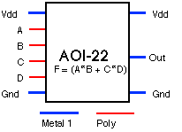
When viewed as a black box, the resulting cell layout should look
something like the one shown below. The top and bottom of the
cell should be bordered by Vdd and Gnd signals, respectively,
which should feed through the cell to allow connection by abutment. The
cell should have four inputs A, B, C, and D, all on the Poly layer (you
may need to use the Metal 1 or Metal 2 layers with appropriate
contacts to "jumper" these signals when creating the layout).

Prelab
- Design and draw a schematic diagram for the AOI-22 gate. Note
that you need to design both the n-transistor "pull-down"
network and p-transistor "pull-up" network, which should
be a dual of the pull-down network as discussed in class.
- Draw up a truth table which shows output values of the AOI-22
gate for all values of A, B, C, and D (there are 16 combinations
of values).
- Using colored pencils
or pens, draw a Stick Diagram of a possible layout for the AOI-22 gate
following the "layout guidelines" given
on the next page while you are doing this.
- HAND IN at the beginning of lab a copy of your schematic, truth
table, and stick diagram developed in the previous 3 steps.
In the Lab
- Use the "magic" layout editor to create a layout
of the AOI-22 gate. Make sure to follow the Layout Guidelines
given below.
- Measure the area of your circuit by selecting the entire cell and
typing "b"
(this macro reports the current dimensions of the Magic "box", which
after
selection is the bounding box of your cell). Be sure to note the
dimensions and
overall area of your cell in your lab report.
Report
For your lab report, hand in the following items:
- A short "Technical Memorandum" which describes (a) your approach
to creating your
AOI gate layout, (b) the characteristics of your layout, including
dimensions and area, (c) any
difficulties you encountered, and (d) suggestions for improving this
lab in the future, if any.
- Your schematic diagram of an AOI-22 gate and truth table.
- Your stick diagram of your planned layout.
- A plot of your magic layout of the AOI-22 gate. Note the
size of the cell on your plot.
Layout Guidelines and Constraints
When designing your layout, you should:
- Include a Vdd! bus at the top of your layout and a Gnd! bus
at the bottom. Note that the "!" character is important,
since it signifies to Magic that this is a global symbol, i.e.
a symbol that is the same throughout a cell hierarchy.
- Include one substrate contact for each connection between
a transistor and a power bus.
- Inputs should be on the left side of the cell and should be in
the order given above. Inputs may use either metal or poly layers.
- Use minimum-size (2-lambda by 3-lambda) N transistors and
"double-wide" (2-lambda by 6-lambda) P transistors for the
time being. We will discuss transistor sizing in more detail later.
- Design assuming an N-Well manufacturing process, and explicitly
draw an N-Well layer in Magic that includes all of your P-transistors.
Magic will automatically create N-Well regions, but it is better
to define the overall well yourself.
- Attempt to minimize the height of the cell, as well as its
overall
area.

